Two-dimensional materials have extraordinary properties such as extremely-low resistance or highly-efficient interactions with light. However, they are inherently fragile.
‘Target identified’:
teaching a machine how to identify imperfections in 2D materials
Applying machine learning to automated characterisation of atomically-thin materials
Just as James Cameron’s Terminator-800 was able to discriminate between “clothes, boots, and a motorcycle”, a FLEET study demonstrates potential for machine learning to identify different areas of interest on 2D materials.
The simple, automated optical identification of fundamentally different physical areas on these materials (e.g. areas displaying doping, strain, and electronic disorder) could significantly accelerate the science of atomically-thin materials.
Atomically-thin (or 2D) materials, including metals, semiconductors, insulators, and more-exotic quantum materials such as topological insulators, superconductors and ferromagnets, are studied by scientists around the world seeking to take advantage of their unique properties.
Materials scientists have utilised this monolayer ‘zoo’ to construct next-generation, energy-efficient electronics, batteries, memory cells and photodiodes.
“Without any supervision, machine-learning algorithms were able to discriminate between differently perturbed areas on a 2D semiconducting material,” explains lead author Dr Pavel Kolesnichenko (Swinburne University of Technology). “This can lead to fast, machine-aided characterisation of 2D materials in the future, accelerating application of these materials in future technologies.”
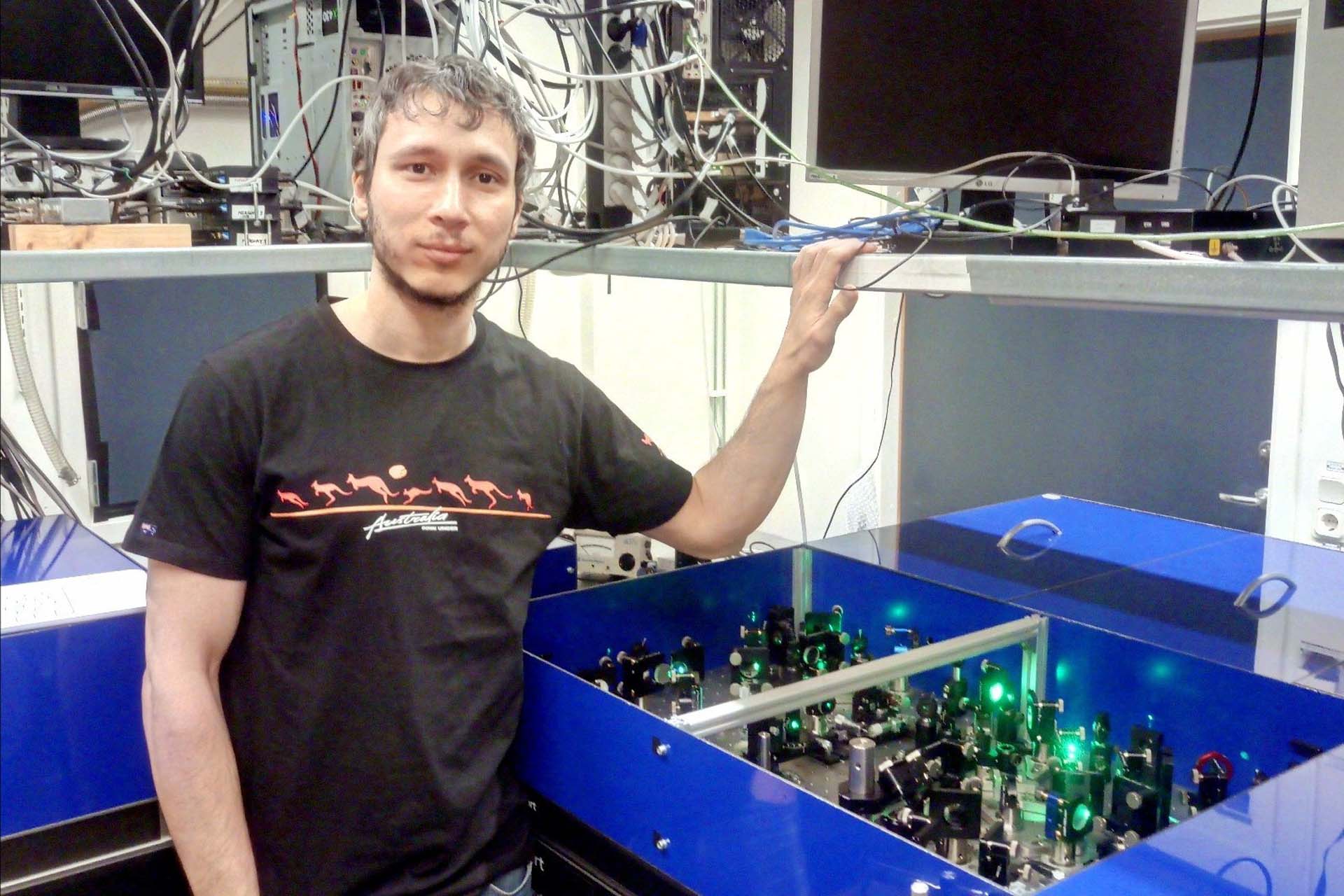
The study was led by Dr Pavel Kolesnichenko at Swinburne University of Technology (and now a postdoc at Lund University)
However with the integration of 2D materials into next-generation technologies still involving mostly manual assembly in one-off prototypes, there is still a long way to go to reach industrial-scale production and commercialisation.
Factors that have hindered progress include lack of full control over materials fabrication, the need for experienced oversight of complex characterisation techniques, and the extreme sensitivity of monolayer materials to perturbations, many of which are introduced unintentionally.
Understanding these perturbations is a non-trivial task, as they can have a combined effect and have to be disentangled.
“So many factors can affect opto-electronic properties of 2D materials, including the type of substrate, additional doping, strain, the presence of wrinkles, defects, and environmental molecules – you name it,” says Pavel.
Pavel and Prof Jeff Davis (also at Swinburne) realised that the laborious task of 2D materials characterisation could be accomplished by machines in a rapid and automated manner.
Working with FLEET colleague Prof Michael Fuhrer (Monash University), they applied unsupervised machine-learning algorithms to characterise the semiconducting monolayer tungsten disulphide. The learning algorithms were able to discriminate between the areas on a monolayer flake affected by doping, strain, disorder, and the presence of additional layers.
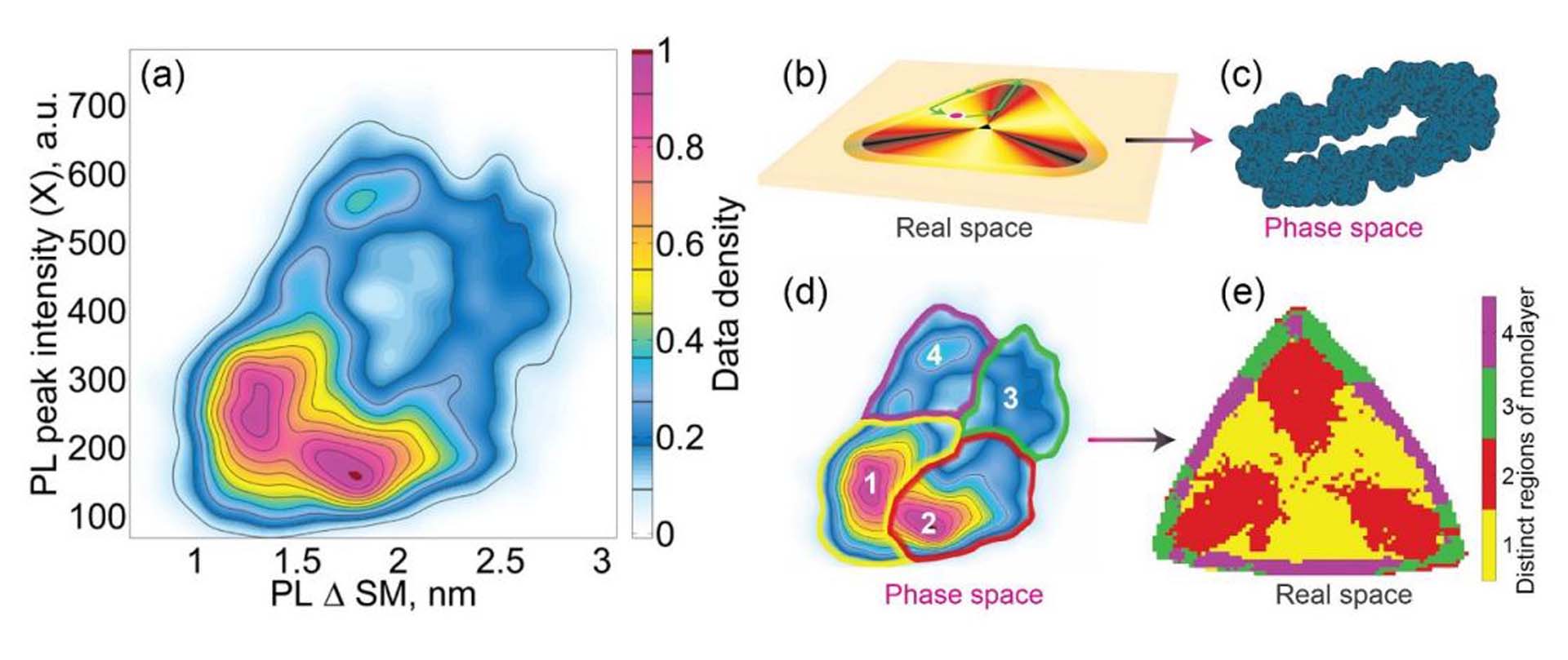
Correlations between experimental parameters help identify specific imperfections causing variations in optical and electronic properties of the 2D material
This is the first time such a systematic disentanglement of these perturbations has been performed.
The team built on previous scientific results in the field including previous work at FLEET, where they disentangled perturbations using correlated photoluminescence and absorption spectra.
In the era of data-driven science and technology, the authors hope that their research will motivate the creation of a large labelled dataset, where labels (such as ‘doping’, or ‘strain’) would be assigned by experienced researchers. This dataset would be then used to train deep neural networks to characterise 2D materials in a fraction of a second. The researchers believe that their work will help to introduce standards for characterisation of monolayer matter, approaching the moment of large-scale use of low-energy smartphones and computers in the future.
This research relates to FLEET milestone M3.1.2.
See page 19 of the strategic plan.
The study was published in Nature Communications in September 2021 (See publications).

We hope this research will motivate scientists to apply similar ideas to other 2D materials and using other imaging modalities..
Dr Pavel Kolesnichenko (Swinburne) FLEET Research Fellow
Collaborating FLEET personnel
Research Fellow
Pavel Kolesnichenko
Swinburne University – alum
Research Fellow
Changxi Zheng
Monash University – alum

Chief Investigator
Michael Fuhrer
Monash University

Chief Investigator
Jeffrey Davis
Swinburne University